Crystal Orientation Dependence of Macropore Growth in
n -Type Silicon
Silke Rönnebeck, J. Carstensen, S. Ottow and H.
Föll
Faculty of Engineering
Kaiserstr. 2
24143 Kiel
Germany
The dependence of macropore formation in n-silicon on substrate orientation was investigated. Samples were cut from a large Si crystals in various orientations between {100} and {111}. Macropores were obtained by electrochemical etching in diluted HF following standard techniques. The growth direction of the macropores was found to be <100> and <113>, with a switch over at a critical angle of about 43°, whereas "break-through" pores obtained without illumination at large field strength always grow in <100>. The results can be partially understood by postulating different pore growth speeds for <100> and <113>, but indicate that a detailed understanding of pore growth in Si is still elusive.
Porous Silicon, produced by anodic dissolution of Si in suitable electrolytes, has received much attention since the discovery of quantum wire effects and strong photoluminescence (PL) in one particular kind of porous Silicon (nanoporous Si) in 1989 1,2. A large body of work was dedicated to the detailed mechanism of the PL and to the production of stable light emitting devices from porous Si - so far without totally conclusive results 3,4. Far less work was dedicated to the formation mechanisms not only of nanopores, but of all types of pores that can be produced by anodic dissolution in Si. At present, several kinds of pores must be treated separately, because no clear connection between their formation mechanisms (as far as they are known or surmised) has been published.
Several formation mechanisms have been proposed, but, to the best of our knowledge, no predictions with respect to the orientation dependence of macropores pores in n-silicon investigated in this paper have been made.
According to the "quantum wire" pore formation model, nanoporous Si must necessarily be formed (also in connection with other pores) if a few requirements are met 5, because then the holes needed for any dissolution process cannot enter the quantum wires and thus no dissolution can occur. However, this model only accounts for nanopore formation in general but has nothing to say about the orientation dependence of the macropores in question.
The "current focusing by bent space charge regions" 6, assumes that current is focused on pore tips because of the bending of the space charge region around the tip. The model certainly has a valid point for the formation of macropores in n-type Si, especially for the regular pore arrays shown in 7, because based on this model and additional empirical results it is possible - within limits - to produce pore structures as desired. The model accounts quantitatively for macropore diameters in n-type Si with prestructured nuclei. However, recently it was found that it can not be applied to heavily doped n-Si 8. Since the shape of the space charge region does not depend on crystal orientation, no influence of the crystal orientation on pore formation would be expected.
The "field induced break-through" model 9 assumes that at some pore tips the electrical field strength is sufficient to allow avalanche break through with the effect that a pore tip - and only a pore tip - can directly generate the carriers needed to facilitate its growth. The model quite obviously accounts for "pure" break-through pores obtained, e.g. with n-type Si at high voltages in complete darkness. But so far it has little predictive power apart from the obvious feature that the pore diameter must be fairly small (» 100 nm and below). Whereas it is not impossible that the field-induced generation of carriers is orientation dependent, no clear predictions result at this point in time.
Models referring to e.g. pore wall passivation 10, diffusion limited random walk 11, or surface instabilities 12,13 are very general (i.e. they would work in any material whenever their assumptions are fulfilled), and so far only provide guide lines for investigations. Their relevance to the orientation dependence of macropores observed in n-Si is not very clear at present.
To summarize: With the present understanding of pore formation in Si no influence of the crystal orientation on pore formation has to be expected as an intrinsic part of existing formation models.
There are, however, a few experimental observations, mostly obtained from investigating {111} oriented samples, that the crystal orientation is important in pore formation. Macropores on {100} surfaces often show more or less pronounced side-pores in <100> directions, and macropores on {111} n-Si substrates were reported to branch in a fractal-like manner in <100> directions 10,14,15, . Only one paper 16 deals with pore growth in other than {100} or {111} oriented substrates and found pores exclusively in <100> directions. The observations, however, were restricted to heavily doped Si which often behaves quite differently from more lightly doped Si. A certain orientation dependence was also found for macropores in p-type Si 17 obtained in water-free acetonitrile, because no pores could be found on {111} oriented surfaces in contrast to pronounced macropores on {100}. This is in contrast to other work on macropores in p-Si 18 , where macropores vaguely oriented in <100> were reported with an acetonitrile based electrolyte.
Since Si specimen with orientations other the {100} and {111} are hard to obtain, samples for experiments were made by cutting slices from a Si crystal endpiece at predetermined orientations with angles of up to 40o between the <100> zone axis and the <111> zone axis (the limit of a custom made goniometer fitted to an ID-saw). After polishing the resulting wafers with diamond paste of 3 µm grain size, specimens with lateral dimensions of 2cm x 2cm were cut from the polished wafers using a conventional saw. For pore etching, the specimens were subjected to anodic etching under conditions identical to those that are commonly used to generate very smooth and well controlled macropores in regular arrays with lithographically defined nucleation. In particular, voltages between 1,5 - 5 V; current densities between 2-5 mA/cm2, electrolyte concentration » 4%, electrolyte temperature 20°C, and samples with nominal resistivities of » 5 Wcm were used; for further details about macropore-formation parameters pertinent to our experiments see 7. Since the results reported in this letter do not depend on the exact values of the experimental parameters listed above, no further details are necessary. The samples were illuminated from the backside and the etching current was kept constant by a controller which adjusted the illumination intensity as outlined in 19 .
In addition to the custom-cut samples, {111} oriented samples obtained from standard wafers were included in the experiments. In the present investigation no prestructured nuclei were used; the diameter of the pores and their average distance therefore fluctuate around average values of about 0.5 µm and 3 µm, respectively. Much information was obtained about the nucleation and growth phase of such "random" macropores 8, suffice it to say that conditions were chosen as best as possible to observe only the phase of stable pore growth.
With the hindsight of the results obtained, a few experiments were performed without any illumination, using only the dark current for etching. The voltage than had to be raised to values of about 40 - 60 V to obtain sufficiently strong currents. In these cases "typical" break-through pores would be expected; i.e. long straight pores with very small diameters.
After cleaving the samples, the pores produced were observed with a scanning electron microscope (SEM). On occasion the sample orientation or the orientation of the cleavage plane was controlled by x-ray analysis. Whereas the orientation was always correct (i.e. as predetermined from goniometer-controlled cutting of oriented crystals), the cleavage plane deviated from the expected {110} plane in a few specimens. The results obtained from these specimens were then discarded. For all micrographs shown in the following figures, the orientation of the cleavage plane is {110}.
Fig. 1 shows typical morphologies of macropores for a {115}and a {112} surface orientation (corresponding to an angle of 15.8o or 35.3o, respectively, between [100] and the chosen orientation). It is obvious that the pores follow the <100> direction in all cases and that side-pores are formed with increasing tendency as the angle between [100] and the surface orientation increases. Whereas the crystallographic direction of the side-pores can not be deduced with certainty from the micrographs, it is at least compatible with <113>, as can be seen from the arrows indicating the <113> and all other relevant directions in Fig. 1 It should be realized that the cross sections shown do not reveal the complete three-dimensional structure of the pores; e.g. side-pores not contained in the cleavage plane are not visible.
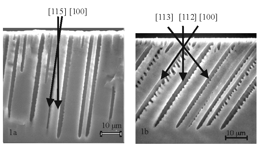 |
Fig. 1a, 1b: The preferential pore growth for backside-illumination on n-typ-silicon wafer with an misorientation of the surface of 15° (Fig. 1a) and 35° (Fig. 1b) to (100). The pores are still growing in [100]-direction. Side-pores are starting to grow in [113]-direction. |
Since it was not possible to cut specimens with misorientations >40o relative to {100}, {111} samples were used. Fig 2 shows typical pores obtained on {111} samples; "typical" refers to an appearance that does not depend very much on the precise etching conditions. Again, the important crystallographic directions are shown as arrows. It is clearly visible that in this case the major pore direction is <113>, a somewhat perplexing result.
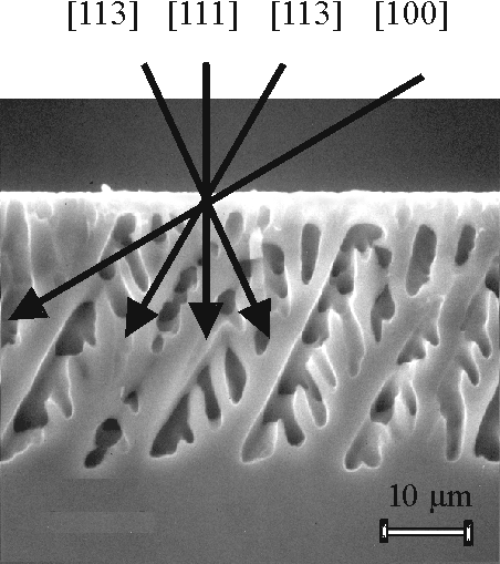 |
Fig. 2: The pore growth on a (111)-surface shows only pores in three equivalent [113]-directions for backside-illumination on n-typ-silicon. |
With the help of stereo micrographs and samples with viewing planes other than {110}, the pore morphology could be worked out in detail; especially the geometry of the side-pores which are more pronounced at larger misorientations.
All observed macropore structures obtained in this way can be understood within the framework of the "current focusing by bent space charge regions" model if two simple assumptions are made:
i) Macropores grow only in <100> and <113> directions.
ii) The growth speed is directly given by the valence n of the anodic processes (the externally measured number of holes needed to dissolve one atom of Si); experimentally we found n » 2.7 for the <100> direction, and n » 4 for the <113> direction. This means that for a given current and pore diameter the pore growth velocity is 4/2.7 » 1.5 times faster in the <100> direction compared to the <113> direction.
The "current focusing by bent space charge regions" model predicts that the pores closest to the backside surface (i.e. deepest in the sample) would collect all the current; it therefore follows:
If the surface orientation of a Si crystal is gradually changed from {100} to {111}, the major pore direction will switch over from <100> to <113> at an angle of » 430, because then pores along <113> grow faster perpendicular to the surface than pores along <100>. This critical angle was just outside of the accessible range in the experiments; its value therefore must be seen as a prediction.
The valence values given above were obtained from relating the approximate pore volume to the total current flow in the various orientations employed in the experiments, they agreed well with the known value of n=2,7 reported for "standard" pores growing in the <100> direction20 .
The unexpected outcome of the orientation dependence of macropores prompted some experiments with "break-through" pores in n-Si; Fig. 3 and Fig. 4 show results. As it turned out, break-through pores are always found along <100> directions and thus are not defined by the direction of the applied field but by the crystallography - another unexpected finding. However, their dependence on crystal orientation is obviously different from regular macropores since no <113> growth directions are observed.
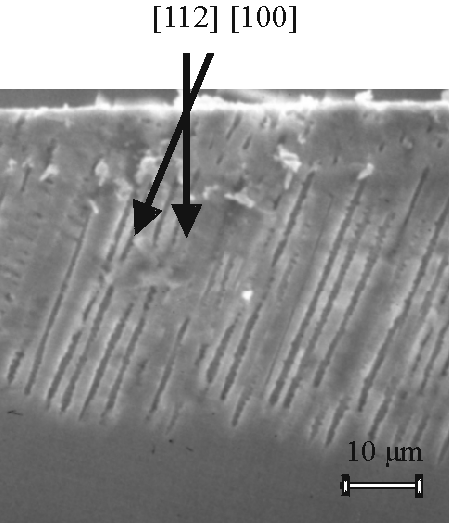 |
Fig. 3: Electric field generated pores on n-typ-silicon without backside-illumination show also a preferential growth in [100]-dircetion. No side-pores in [113]-direction are visible (angle between corresponding directions vary in the Fig. 1 and Fig. 3 because the cleavage plane is not always (110)). |
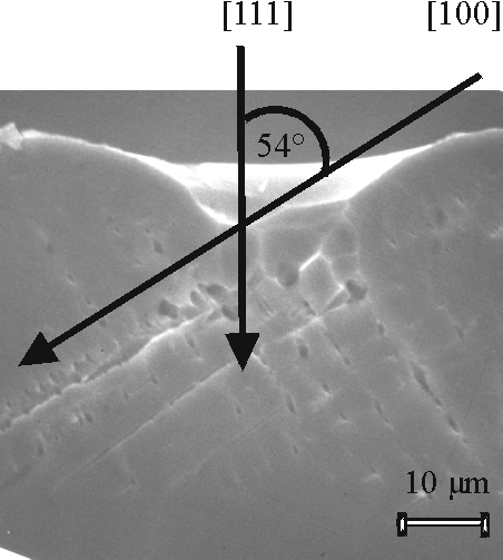 |
Fig. 4: Electric field strength generated pores on (111)-surface on n-typ-silicon are shown. In contrast to the pores with backside-illumination these pores grow in [100]-direction. |
At the time being, the observations must be taken as a direct evidence that pore formation in Si is not well understood. It is clear, of course, that some phenomena implicitly contained within the framework of pore formation models could be orientation dependent, i.e. the energy levels in quantum wires or the critical field strength for carrier generation in an avalanche mechanism. It is also very likely that the bond termination of the Si surface, which differs for different orientations 16,17 , plays a major role in pore formation, but no predictions of the actual behavior seems to be possible at present.
Whereas, to the best of our knowledge, this is the first time that the <113> direction figures in pore formation, {113} planes and directions are known to play a special, if poorly understood role in Si. The so-called {113} defect or stacking fault often observed after irradiation of Si (the nature of which, after much investigation, is still not understood) should be mentioned 21, or the particularly interesting 3x2 and 3x1 reorganization of the (113) surface under UHV conditions 22. Dislocations have been seen aligned in <113> direction and other {113} phenomena are occasionally mentioned in gatherings of silicon experts, but rarely published because of their obscurity. Pore etching thus may be useful to obtain a better understanding of the special role of {113} in Si crystals.
In the light of the present experiments, the older observation of one of the authors 14 of macropore growth along <100> for {111} must be reconsidered. Either <113> pores were actually present, but not perceived since no detailed measurements were made, or the pores were predominantly break-through pores.
If combining all observations relating to macropore formation (including especially the recent finding that holes upon reaching the pore tip do not react immediately with the electrolyte, but will escape with a certain probability until they finally disappear in the chemical reaction 8), we are lead to believe that the basic interface reactions:
i) Direct dissolution (Si + HF + n1h+ Þ SiF2 + 2H+ + (2 - n1) e-) and/or
ii) Dissolution by oxide formation with subsequent purely chemical oxide dissolution (Si +4 H2O+ n2h+ Þ SiO2+ 4 H+ ) 10,23
are very sensitive to the surface orientation expressed in the detailed bonding structure found at the precise site of the reaction. In this context it may be of interest to note that the valence n1is supposed to be » 2, and n2 » 4; and macropore formation is associated with a current density at the pore tip right at the crossover between the two mechanisms with an effective n of » 2.7 20.
Whereas the pore formation shows a pronounced influence on crystal orientation, other measurements undertaken with arbitrarily oriented Si - e.g. the current - voltage characteristics 20 - do not show a very pronounced orientation dependence. This may happen because the specific starting surface is almost instantaneously converted into an "average" type by dissolution and the pores being formed. More subtle effects, however, have been observed. It is, e.g., not well understood why preferential etches composed to delineate defects like dislocations or precipitates are extremely sensitive to the surface orientation. From the many recipes for preferential etches in the HF - CrO3 - CH3OH system, the "Sirtl-etch" 24 works only on {111} surfaces, the "Seiter-etch" 25 only on {100}, and the "Secco-etch" 26 on all planes.
We are grateful to the Wacker-Company for supplying the silicon-crystals and a surplus ID-saw. M. Christophersen help, who supplied some additional data, was essential for the paper. This work was supported by the Deutsche-Forschungs-Gemeinschaft (Förderungsnummer: FO 258/1-1).
2. L. T. Canham, Appl. Phys. Lett., 57, 1046 (1990)
3. A.G. Cullis, L.T. Canham and P.D.J. Calcott, J.Appl.Phys., 82 (3) (1997)
4. J.von Behren, M. Wolkin and P.M. Fauchnet, in Porous Semiconductors- Science and Technology, L.T. Canham and V. Parkhutik, Editors, O-18, p. 38, Extented Abstracts of the International Conference, Mallorca, Spain (1998)
5. V. Lehmann and U. Gösele, Av. Mater., 4, 762 (1992)
6. H. Föll, Appl. Phys. A, 53, 8-19 (1991)
7. V. Lehmann and U. Grüning, Thin Solid Films, 297, 13-17 (1997)
8. M. Hejjo Al Rifai, M. Christophersen, S. Ottow, J. Carstensen and H. Föll, in Porous Semiconductors- Science and Technology, L.T. Canham and V. Parkhutik, Editors, O-06, p. 18, Exented Abstracts of the International Conference, Mallorca, Spain (1998)
9. M.J.J. Theunissen, J. Electrochem. Soc., 119, 351 (1972)
10. V. P. Parkhutik, in Porous Silicon, p. 301, Z.C. Feng and R. Tsu, editors, World Scientific, Singapore (1994)
11. R. L. Smith, S. F. Chung and S.D. Collins, J. Electron. Mater., 17, 533 (1988)
12. Y. Kang and J. Jorné, Appl. Phys. Lett., 62, 2224 (1993)
13. A. Valance, Phys. Rev. B, 52, 8323 (1995)
14. V. Lehmann and H. Föll, J. Electrochem. Soc., 137, 653 (1990)
15. T. Osaka, K. Ogasawara and S. Nakahara, J. Electrochem. Soc., 144, 3226 (1997)
16. M.C. dos Santos and O. Teschke, J. Vac.Sci.Technol.B, 16(4), 2105 (1998)
17. M. M. Rieger and P. A. Kohl, J. Electrochem. Soc., 142, 1490 (1995)
18. E. A. Ponomarev and C. Lévy-Clément, Electrochemical and Solid-State Letters, 1 (1), 42-45 (1998)
19.V. Lehmann, Thin Solid Films, 255, 1-4 (1995)
20. V. Lehmann, J. Electrochem. Soc., 140, 2836 (1993)
21. S. Takeda, M. Kohyama and K. Ibe, Phil. Mag., A 70, 287 (1994)
22. J. Dabrowski, H.-J. Müssiger and G. Wolff, J. Vac. Sci. Technol. B, 13 (B) (1995)
23. O. Nast, S. Rauscher, H. Jungblut, H.J. Lewerenz, J. Electroanal. Chem., 442: 169 (1998)
24. E. Sirtl and A. Adler, Z. Metallkunde, 52, 529 (1961)
25. H.Seiter, in "Semiconductor Silicon 1977", H. R. Huff and E. Sirtl, Editors, p. 187, The Electrochemical Society Softbound Proceedings Series, Princeton, N.J. (1977)
26. F. Secco d´Aragona, J. Electrochem. Soc., 119, 948 (1972)