The atomic density of Si is 4.96 · 1022 cm–3 or about 5 · 1022 cm–3 .
1 ppm thus corresponds to 5 · 1016 cm–3.
[S] = [V] /a with a = lattice constant (= 0,5431 nm) or, more precise for single crystals, distance between the crystallographic planes. With a » 0,5 nm = 5· 10–8 cm, we have
[V] = 5 · 1016 cm–3 = 1 ppm corresponds to S = 108 cm–2.
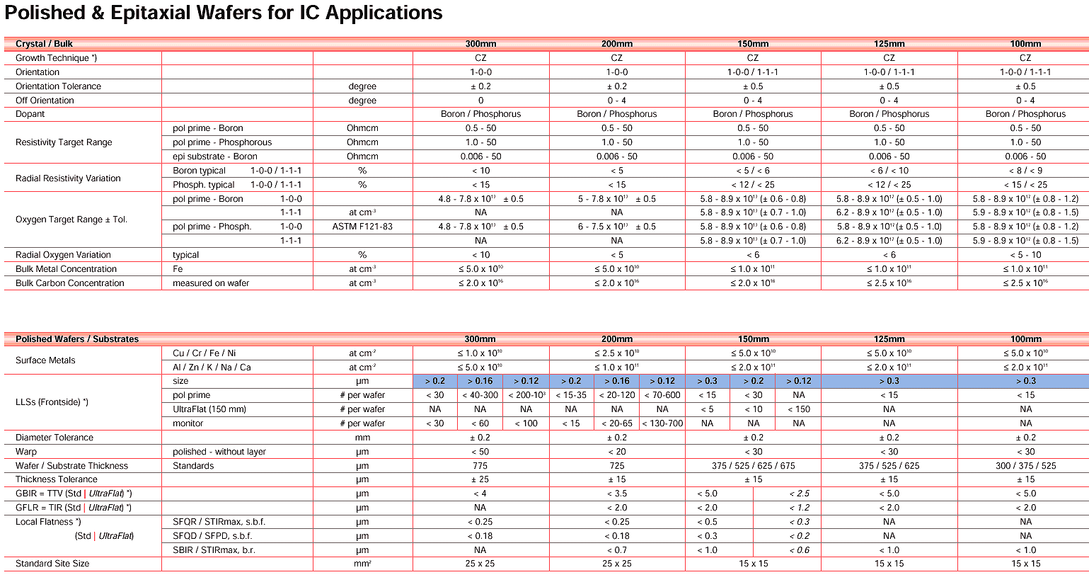
LLS (sometimes also abbreviated LPDs): Localized Light Scattering Defect; this relates to a detection method of sub-µm size surface imperfections (resulting from bulk microdefects)
SFQR: Site flatness quality requirements (??): Definitely a measure of flatness in a region comparable to the size of a single chip
(The rest: Who knows?
http://www.freiberger.com/english/products/geom_parameters.php
 |