 |
 |
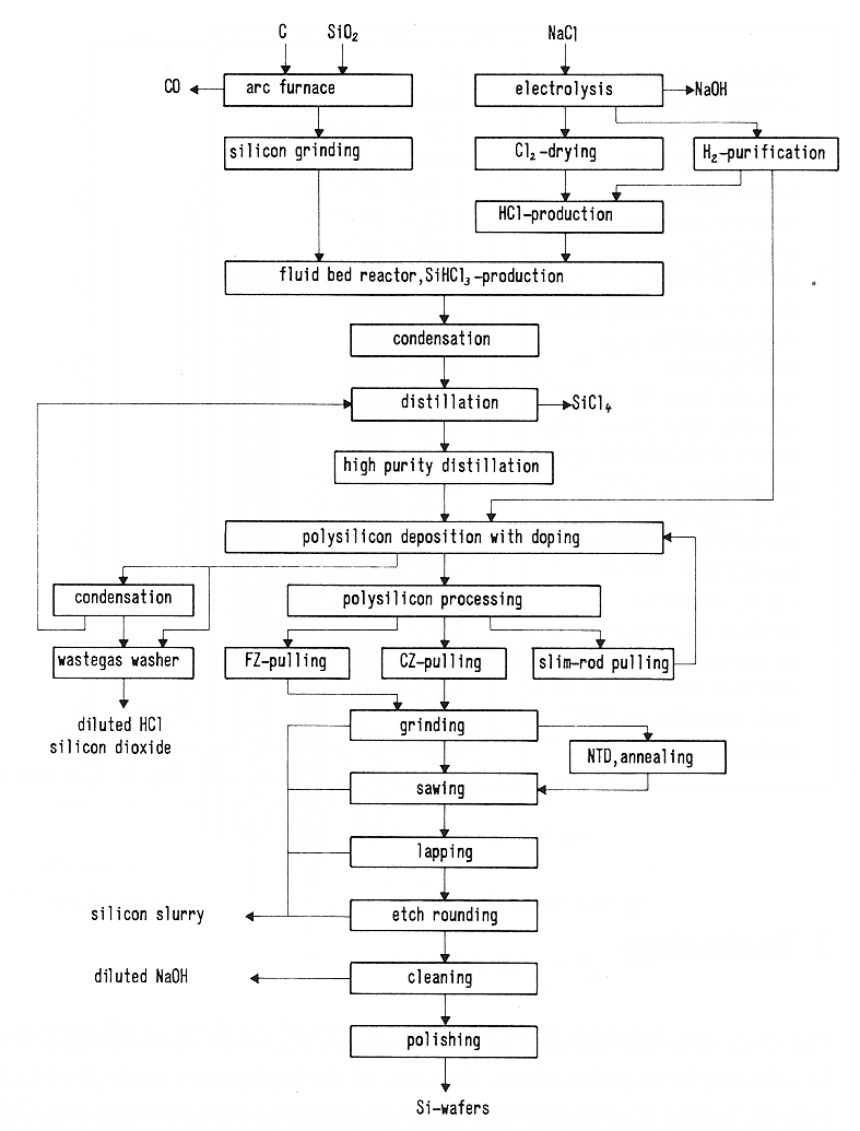
| First a schematic process flow graph is given for everything - from sand to wafer. | |||
| It includes side processes not covered in the backbone modules which, however, are self explanatory. | |||
| |||
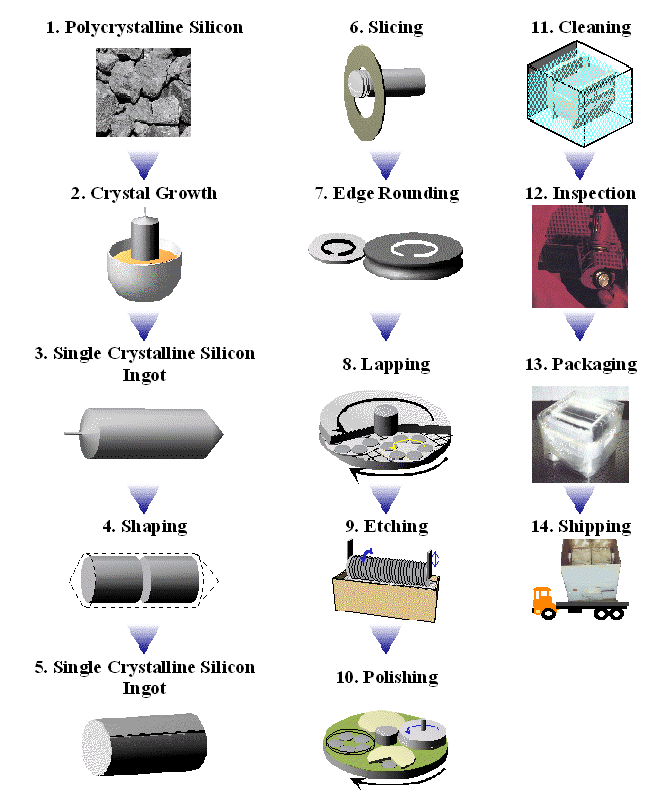
| Next, we have a pictorial representation of just crystal growth and wafer production. Again, it contains some self-explanatory processes not introduced before. | |||
| |||
© H. Föll (Electronic Materials - Script)