 |
Sputter Deposition | |
|
|
 |
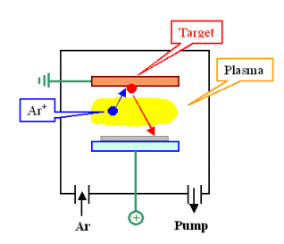
Simple in principle: Shoot off any mixture of atom contained in a target be an
ion beam produced by applying high (RF) voltage between target and Si wafer; see picture. |
|
|
 |
Great advantage is easy deposition of mixtures of elements, e.g. Al plus traces of Cu etc. |
|
|
 |
Disadvantage:
1. target should be conducting; no (easy) deposition of insulators like
SiO2.
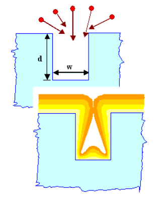
Target atoms are emitted in all directions, leading to: |
|
 |
"Contact hole filling problem" |
|
|
|
 |
The picture tells it all. At some point you need to go back to CVD processes. |
|
 |
Ion implantation. Might be considered to be a "deposition" technique
but actually shoots ions into the Si target. | |
|
 |
The technique of choice for doping selected areas with typically B, As or P.. Depth distribution
and concentrations finely adjustable in a wide range. | |
|
 |
Major problems:
1. The Si crystals gets more or less destroyed; in the extreme it turns
amorphous. Implantation thus always need a follow-up annealing process that changes dopant distribution by diffusion and
may not be able to restore perfectness of the lattice
2. Implanters are huge, complex and very expensive machines. |
|
 |
Other physical deposition techniques.
There are plenty, often quite specialized.
Of special important for chip making are. | |
|
|
 |
Evaporations. Easy but very limited. Rarely used in chip production |
| |
|
 |
Spin-on techniques (for deposition the light sensitive "resist" needed for lithography |
| |
|
 |
Molecular Beam Epitaxy (MBE);: hugely important for III-V technology.
Galvanic techniques.
Hated but used
Many other. | |
|
|
|
|
© H. Föll (Electronic Materials - Script)

