 |
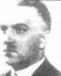
| While everybody in the semiconductor world knows the "Czochralski grown crystals", (almost) nobody knows Jan Czochralski . | ||
| He was born 1885 in Kcynia, a small town in Western Poland, which then was part of Prussia; i.e. the German empire. Around 1900 he moved to Berlin, 1907 he worked as an engineer for the "Allgemeine Elektrizitäts Gesellschaft (AEG), a formerly large and famous company, defunct since about 1980 (the last remnants were swallowed by Daimler-Benz). During this time he also studied Chemistry and Metallurgy at the "Charlottenburg Technical University" and Fine arts at the Berlin university. | ||
| 1917 he organized the well-equipped research laboratory of "Metallbank und Metallurgische Gesellschaft"; and he was the director of that institution until 1928. | ||
| 1929 he moved back to Poland to become a Professor of Metallurgy and Metal Research in in the Chemistry Department of the Technical University in Warsaw. | ||
| All the time he was involved in metallurgical research, active in many scientific organizations and advising companies and other professional entities. The second world war put an end to all this - J. Czochralski was active in supporting his co-workers and the polish underground army. | ||
| After the war he returned to his native town of Kcynia were he run a small drug firm. He died in 1953 and is buried in the family tomb in Kcynia. | ||
| He was quite well-known for many contributions in metallurgy, especially for this studies of the velocity of metal crystallization, and, of course, for his method of monocrystalline growth, published in 1916. | ||
| "Czochralski grown crystals" are a cornerstone of modern material science, and J. Czochralski will be remembered for his insights leading to this method. | ||
| But like many scientists, he was also interested in literature, music and painting and not afraid of branching out, as witnessed by his activities after the war. | ||
|
|
He is one of the most famous Polish scientists and the Foundation for Materials Research Development in Poland established the Prof. Jan Czochralski Gold Medal for achievements in materials science. | |
| Note added after consulting an Internet article from Dr Pawel Tomaszewski. (http://rekt.pol.lublin.pl/~ptwk/art2.htm ) | ||
| What I did not know was that the discovery of the Czochralski crystal growth methods was one of those accidental discoveries; here a quote from the article mentioned above | ||
| "DISCOVERY OF THE CZOCHRALSKI METHOD The Czochralski method of growing single crystals brought Jan Czochralski his greatest publicity. The method was developed in 1916 and was initially used to measure of crystallization rate of metals. The method was developed as a result of an accident and through Czochralski's careful observation. One evening he left aside a crucible with molten tin and returned to writing notes on the study carried out on a crystallization study. At some moment, lost in thoughts, instead of dipping his pen in the inkpot, he dipped it in the crucible and withdrew it quickly. He observed then a thin thread of solidified metal hanging at the tip of the nib. The discovery was made! The nib slot, in which crystallization was initiated, was replaced by a special narrow capillary and in some cases by a seed of the growing crystal. Czochralski checked later that the crystallized wire was a single crystal. The crystals obtained in that way had diameters of about a millimeter and lengths up to 150 cm. Czochralski published a paper on the study of the rate of crystallization of tin, zinc and lead, and the maximum rate of pulling of a crystal was recognized as the characteristics of the crystallizing material (Ein neues Verfahren zur Messung des Kristallisationsgeschwindigkeit der Metalle [A new method for the measurement of crystallization rate of metals], Z. phys. Chem. 92, 219-221 (1918); the paper was received in the editorial office on 19 August 1916)." | ||
© H. Föll (Electronic Materials - Script)