 |
After much designing, simulation, process trials and test chips comes the moment when the first
product chip containing the new generation will enter the line and becomes processed. Processing may take several month
because many processes do not work too well or are done in prototype machinery. Here is a real example from the development
of a 16 Mbit DRAM at Siemens. |
|
 |
If the batch of wafers does not die a sudden death at some shaky process (or because somebody
simply drops them), "First Silicon" will eventually emerge. This is a big moment
in the life of the team - now we will see if several 100 man years and many million $$ were well spent.
|
|
 |
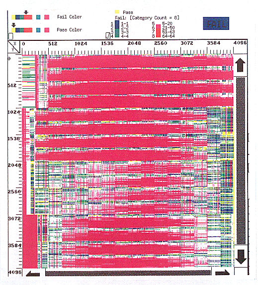
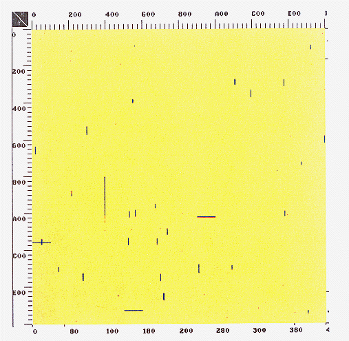
The test crew starts to measure the function of the memory with the chips still on the wafer.
The results are plotted in a matrix mimicking the matrix of memory cells on the chip. The color given to a pixel encodes
the quality of the individual memory cell. Yellow means fully functional, all other colors, especially red, mean trouble. |
|
 |
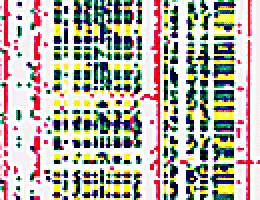
Below is a plot for the best chip from the "first Silicon". The insert on the right
shows that single pixels are resolved in principle. How was the feeling with a result like that? |
| |
|
|
|
 |
The feeling was : Get out the champagne! There are fully
functional memory cells on this chip! Not too many - but who cares. This was good! More often than not, nothing whatsoever
works on first Silicon. A few hundred cells that work are enough to measure all critical parameters of the circuits and
to get the desperately needed data for optimizing design and processes. |
 |
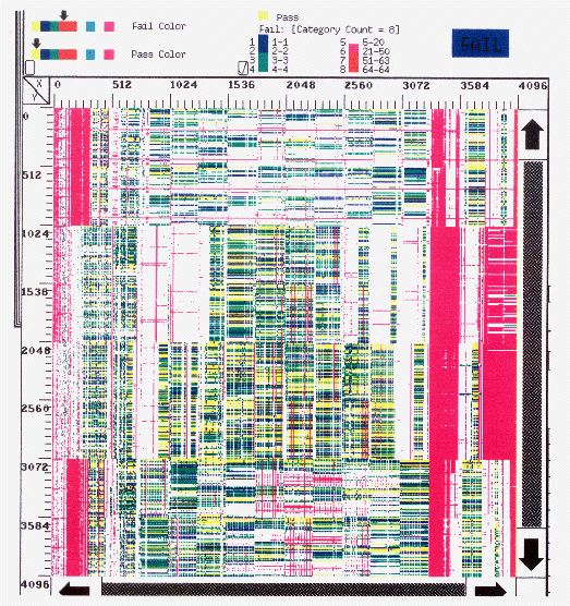
Next comes second Silicon. Those wafers probably were processed
to some degree when first Silicon came out, so only back end processes can now be optimized. But there is improvement: A
little bit more yellow, but far less deep red! |
|
 |
The structure in these plots - pixels of the same color arranged in lines - simply reflects
the fact that a number of memory cells share the same bit- or word line. If this line is interrupted, all its memory cells
fail. |
| |
|
 |
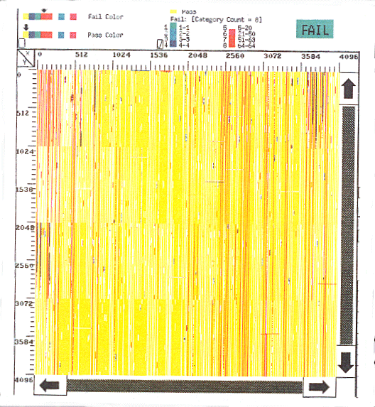
Here we have the first redesign - all the things learned from first Silicon are now incorporated
into the chip. |
|
 |
And now the yellow color dominates. While this looks pretty good, we are still a million or
so cells short of total success. |
| |
|
 |
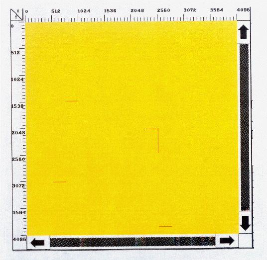
Now the process stabilizes and a new game starts: Get rid of the few but noticeable problems
in the memory matrix. This is tough! |
| |
|
 |
Now we won: Only a few strongly correlated failures - no single bit problems. This can be solved
- with luck - by activating some redundant memory cells that will take over the function of the failed cells |
| |
|
 |
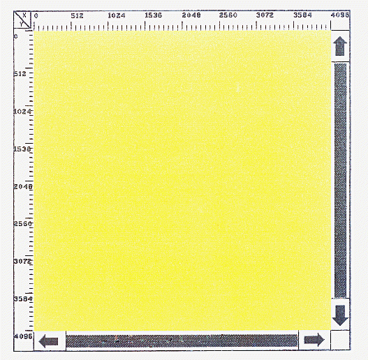
Triumph!! Using the built in redundancy, a fully functional memory matrix was obtained for
the first time - in the third full process cycle, a very good score. |
|
|
|
 |
Exactly two chips out of some thousand candidates are fully functional. The project goals have
been met. |
 |
All that remains to be done now is to crank up the yield to, say, 15 % functioning chips
per wafer so that production can start. |
|
 |
That was a joke: Now the really hard
work starts. It will take considerably more time and money to "just improve the yield" than it took to get to
this point in the chip development. |
| |
|
© H. Föll (Electronic Materials - Script)
![]() 5.4.2 Working in Chip Development and Production
5.4.2 Working in Chip Development and Production