 |
Typical wafer size for new factories (2007) : 300 mm diameter, 775
µm thickness, flatness in lower µm region | |
|
|
 |
Chip size a few cm2, much smaller if possible |
|
|
 |
Yield Y = most important parameter in chip production = % of chips on a wafer
that function (= can be sold). | |
|
 |
Y = 29 % is a good value for starting production |
|
 |
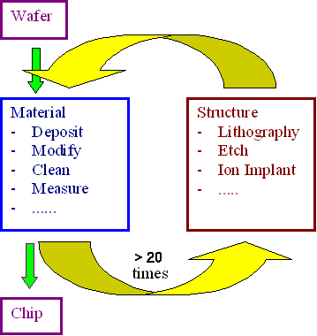
Chip making = running about 20 times (roughly!!) through "materials"
- "structuring" loop. | |
|
 |
About 400 - 600 individual processing steps (= in / out of special "machine")
before chip is finished on wafer | |
|
 |
More than 30 processing steps for packaging (after separation of chips by cutting) |
|
|
 |
Simple estimate: 99.9% perfection for each processing step meansY < 70
%. | |
| |
| |
| |
© H. Föll (Electronic Materials - Script)
