 |
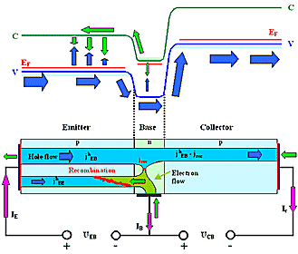
Essentials of the bipolar transistor: |
|
|
|
 |
High emitter doping (NDon for npn transistor
here) in comparison to base doping NAc for large current amplification factor g
= IC/IB. | |
|
 |
NDon/NAc »
k = injection ratio. | |
| | |
| |
| |
| g | » |
NDon
NAc | · |
æ
ç
è | 1 – |
dbase
L | ö
÷
ø
|
|
| |
|
| |
|
|
 |
Small base width dbase (relative to diffusion length L)
for large current amplification. | |
|
 |
Not as easy to make as the band-diagram suggests! |
|
|
| |
| |
 |
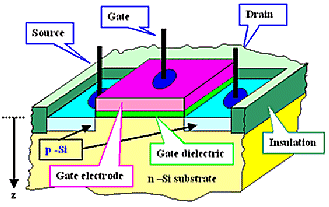
Essentials of the MOS transistor: |
|
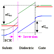
 | | Band diagram for inversion |
|
|
 |
Gate voltage enables Source-Drain current |
|
|
 |
Essential process. Inversion of majority carrier type in channel below gate by:
- Drive intrinsic majority carriers into bulk by gate voltage with same sign as majority carriers.
- Reduced majority concentration nmaj below gate increases minority carrier concentration nmin
via mass action law
| |
| | |
| |
| |
| |
|
|
|
- An inversion channel with nmin > nmaj develops below the gate as soon
as threshold voltage UTh is reached.
- Current now can flow because the reversely biased pn-junction between either source or drain and the region below
the gate has disappeared.
| |
| | |
| |
|
 |
The decisive material is the gate dielectric (usually SiO2).
Basic requirement is: | | |
|
 |
High capacity CG of the gate electrode - gate dielectric -
Si capacitor = high charge QG on electrodes = strong band bending = low threshold voltages
UG | |
|
|
 |
It follows:
- Gate dielectric thickness dDi
Þ High breakdown field strength UBd
- Large dielectric constant er
- No interface states.
- Good adhesion, easy to make / deposit, easy to structure, small leakage currents, ...
|
|
Example:
U = 5 V, dDi = 5 nm Þ E = U/dDi
= 107 V/cm !!
er(SiO2) = 3.9 |
|
© H. Föll (Electronic Materials - Script)


