 |
With the ELYMAT
(a special technique to map minority carrier lifetime in Si; see the publications in the link), D-defects
and other microdefects in Si can be "seen" in some cases because they decrease the minority carrier life
time (they act as recombination centers). |
|
 |
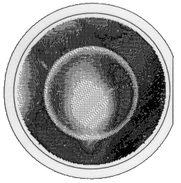
The pictures obtained monitor the local photo current (induced by a scanned Laser
beam) in special electrolytic junctions. It is a direct measure of the minority carrier life time. A typical picture of
state-of-the-art as-grown 150 mm Si wafers from around 1990 is shown below. Bright areas correspond to decreased
life times. |
| |
|
|
 |
The most outstanding feature is the well-defined ring. It is due to small defects incorporating SiO2. |
|
 |
With hindsight gained by much research in the nineties, the situation is as follows: Inside the oxygen-precipitate
ring, small vacancy agglomerates (in the form of octahedral little voids) dominate; outside the ring, interstitials agglomerates
(probably in the form of small stacking faults and dislocation loops (the old "classical" swirl defects)) were
formed. |
 |
This rather unique defect pattern is the result of the complicates interaction of three main
point defects: vacancies, Si-interstitials and O-interstitials. Whereas the above interpretation is now universally
accepted, the details about the primary defects are not yet known beyond reasonable doubt. |
|  |
For a recent review read the paper of Bob
Falster and V.V. Voronkov. |
| | |
© H. Föll (Defects - Script)

![]() 1.3.3 The larger View and Complications
1.3.3 The larger View and Complications