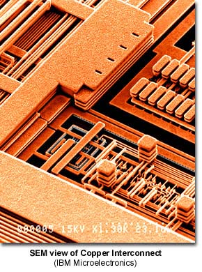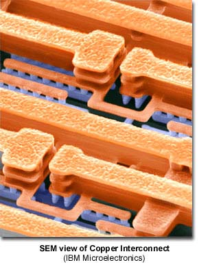

Copper conducts electricity with about 40 percent less resistance than aluminum which translates into as much as a 15 percent speed increase in microprocessors that use copper conductors. In ultra-small chips at high current densities, copper is also far less vulnerable than aluminum to electromigration (the movement of individual atoms through a conductor, caused by high electric currents) which creates voids and ultimately breaks conductors.
Why hasn't the industry already adopted copper? Copper has long been considered a semiconductor killer. Not only does copper rapidly diffuse into silicon, but it changes the electrical properties of silicon in such a way as to prevent the transistors from functioning.


IBM has finally overcome these obstacles with a key technology for patterning copper called Damascene. This is a reference to the metallurgists of old Damascus who produced the finest polished swords in the medieval world. IBM first used this technique to form "vias" - the small metal plugs that link separate layers of wiring in chips.
In conventional deposition, a layer of metal and photoresist are deposited on a silicon wafer. Unwanted metal is then etched away with an appropriate chemical, leaving the desired pattern. Next, the spaces between the wires or vias are filled with silicon dioxide, and finally the entire wafer surface is polished to remove excess insulator.
Damascene patterning involves the same number of steps, but reverses the order of deposition. The pattern of wires or vias is first formed by etching the oxide. The metal is deposited second, and the excess is removed by polishing. In both conventional and damascene patterning the process is repeated many times to form the alternating layers of wires and vias which form the complete wiring system of a silicon chip.
To overcome copper's tendency to diffuse in silicon, IBM devised a means of depositing a complex copper structure on polyimide, a compound used as an electrical insulator in silicon chips.
Address comments or problems to webmaster@fullman.com
