| |
Transmission Electron Microscope (TEM) |
|
The High-Voltage Transmission Electron Microscope (HVTEM) |
 |
FFor my PhD thesis I used a “Hitachi HU 650” High-Voltage Transmission
Electron Microscope (HVTEM) that employed 650 kV. It was the pride and joy of the
Max-Planck-Institut für Metallforschung; the only HVTEM in Germany and one of two found in Europe. No. 2, if memory
serves, could be found in Toulouse, France. Our HVTEM was equipped with a custom-built He cooled low temperature specimen
stage, and that made it rather unique. |
| |
 |
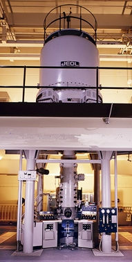
It is thus a bit surprising that you can’t find a picture of the microscope
in the Internet. It wasn’t easy to photograph since it was 2 stories high, but still. I therefore can only give you
a picture of a competing JEOL HVTEM. Our Hitachi wasn’t much different. |
| | |
|
| |
|
 |
| A JEOL HVTEM |
|
| | |
 |
You only see the microscope column and the high-voltage tank on top. What you
don’t see are many big cabinets containing the (vacuum tube) based electronic, the pumps for producing the for needed
vacuum, the contains where the SF6 was kept when it wasn’t filling the high-voltage tank, the water-cooling
circuits and implements, and the liquid nitrogen tank needed filling the cooling traps in the vacuum system. Not to mention
the big box full of tools we needed we we took the whole thing apart - down to the last screw if necessary - for cleaning
and repairs. And for that you needed a big crane hovering over the whole contraption. It was a big thing, in other words.
|
| |
 |
Nowadays it is hard to belie that students doing diploma or PhD work were allowed
to take something like this microscope apart, or to fool around with a soldering iron in the electronics. But remember (or
learn): there were no integrated circuits and in particular no software. The word “software” hasn’t even
been invented yet. With some background to the working of vacuum tubes and transistors one could understand the circuit
diagrams and venture to make repairs or even improvements. |
| |
|
|
The Siemens Elmiskop 102 |
 |
The Siemens Elmiskop 102 hit the market in 1973. The MPI Stuttgart bought one
- for roughly 250.000.- DM (about 125.000.-) - in 1975 / 76. I didn’t use it much and I did not know that it could
be coerced to deliver atomic resolution; at least with Si specimen at 0,31 nm lattice spacing. Siemens, I must presume,
didn’t know that either otherwise they would have told us. |
| |
 |
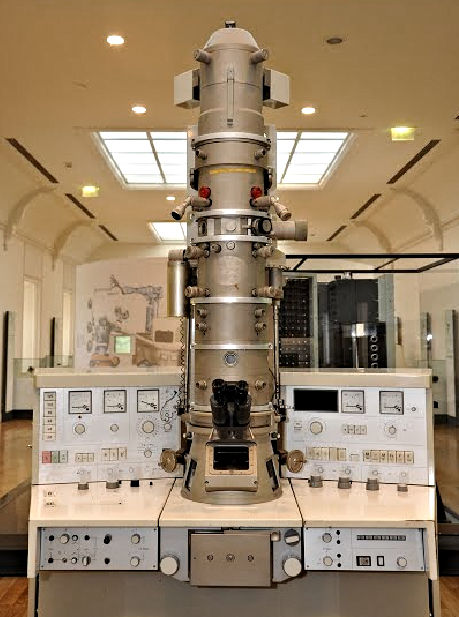
Here is the Elmiskopo 102 |
| | |
|
| |
|
 | | The ELMISKOP 102 |
|
| | |
|
 |
Not visible is the high-voltage tank (delivering a measly 125 kV) and the primary vacuum pumps.
The microscope is obviously an analogue device. No software, no screens, perhaps a few early integrated circuits. The electronics,
however, contained mostly transistors and only a few special vacuum tubes. The Elmiskop at Cornell was pretty much the same
kind of machine and it could do high-resolution work. That is mostly due to the expert maintenance by Ray Coles and some
small improvements I had made (with Ray’s help) at the electronics concerning beam tilting |
 |
If you want to learn more about (electron) microscopy, usethis link. |
| |
|
© H. Föll (Archive H. Föll)

![]() 3.1 TEM Work at Cornell University; 3.1 TEM Investigations of Grain Boundaries in Silicon
3.1 TEM Work at Cornell University; 3.1 TEM Investigations of Grain Boundaries in Silicon